Edsim51 Tutorial Pdf
The Peripherals:. ADC. Comparator. Four 7-segment LED Displays.
LCD Module. UART. Keypad. LED Bank. Bi-directional Motor.
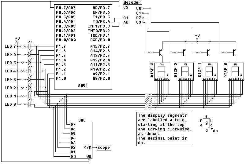
Switch Bank. DAC (output displayed on oscilloscope)Theseimage on the left shows what is connected to each of the 32port pins. If a pin's description is too long to fit, you can see thefull description by hovering the mouse over it, or by clicking on thezoom button (see below).ZoomClick on one of the buttons marked + to display thatport's connections in a separate window. An example for port 2 is shownbelow.Port Pin ConnectionsThe logic diagram below gives details of the peripheralinterfacing.EdSim51 Simulator Peripheral Logic Diagram. The LED Bank, DAC and the 7-segmentDisplaysAs can be seen in the diagram below, the LED bank, the DACinputs and the 7-segment display data lines all share port 1.The selection of which of the four displays isenabled is done via P3.3 and P3.4.
Edsim51 Tutorial Pdf 7,1/10 9781votes. Robert Yates Serial Killer Wife. Do you want to learn about microcontrollers and embedded systems? The EdSim51 simulator can only parse assembly programs. It cannot compile C programs, therefore do not try to copy and paste the program below into EdSim51. Instead, you should compile the program in uVision3 and use the Intel HEX output file. This type of file can be loaded into EdSim51. See notes on EdSim51 and Intel HEX files.
These port pins are applied to a2-to-4 line decoder, the outputs of which are applied to the base oftransistors that enable/disable the displays.Logic diagram showing the LED bank, DAC and7-segment display connections only.The decoder is enabled via a logic 1 on P0.7. Thispin is also applied to the DAC WR input, which is active-low.Therefore, to write data to the DAC the programmer disables thedisplays, which also has the effect of enabling the DAC's data lines.Data can then be written to the DAC.
Whatever is on the inputs when theWR line is taken low is stored in (or written to) the DAC's internalregister and remains there after the WR line is taken high. Theanalogue output for this data will be displayed on the scope until thenext time WR is taken low and a new value is placed in the internalregister.The keypad can beimplemented using the external interrupt 1 line (see ), but not while alsomultiplexing the 7-segment displays.
This is because the externalinterrupt 1 line (P3.3) is also used by the display decoder (see logicdiagram above). Therefore, keypad interrupt and multiplexing the7-segment display cannot be used at the same time - the keypad AND gateshould be disabled.An example of the DAC in action is shown below. LED Bank and the7-segment Displays PanelThe code that generated the above ramp is alsoshown (above middle). The DAC's WR input is taken low permanently ( CLR P0.7)while the value in the accumulator is sent to the DAC's inputs,increased by 8 and then sent to the inputs again, and so on.When the mouse is placed over the scope screen, a tooltip appears,stating the scope's vertical scale is one volt per division and the horizontal scale is, in this case, 25microseconds per division. The scope's horizontal scale is tied in with the 8051 systemclock frequency (this is unrealistic, but I feel it's adequate forsimulation purposes). If, for example, the system clock frequency ischanged to 11.059 MHz, then the scope's horizontal scale is 17.36 microseconds perdivision.
4-bit Mode: TheLCDmoduleisasimulationofthe Hitachi HD44780 and is interfaced to the 8051 in 4-bit mode.P1.7 through P1.4 are connected to DB7 through DB4, while P1.3 isconnected to the register-select pin and P1.2 is connected to theenable pin. Notice the read-write pin is connected to ground - themodule can only be written to.8-bit Mode: By default, as stated above, the module isinterfaced in 4-bit mode. However, the lower four data bits (DB3through DB0) are also available (on P1.3 through P1.0). If the userwishes to write to the module in 8-bit mode, RS and E should beremapped to other port pins, using the DI button at the top left of the peripheral panel.Details of the pin functions and theinstructions for the LCD module are given below. For details on how tocommunicate with the module, see and some.Reading:Instructions for reading from the module have not been implemented.CharacterBlinking: Because the simulator does not run in real-time, itwould be hard to know if the module was blinking. Therefore, if theprogrammer sets the module to blinking (see Display on/off control instructionbelow), the cursor position character alternates between blue text withred background and red text with blue background. In this way theprogrammer knows at a glance if the module is in blinking mode (whennot in blinking mode, all characters are black with grey background).The enable pin (E,connected to P1.2) is negative-edge triggered.
On a negative-edge on E,the module reads the data lines DB7 - DB4.4-bit Mode: Ascanbe seen in the logic diagram above, the module is interfaced with the8051 in 4-bit mode. In 4-bit mode, the module's lines DB3, DB2, DB1 and DB0are not used. The 8-bit instruction or data must therefore be sent intwo 4-bit nibbles.
The high nibble is sent first, followed by the lownibble. When the enable pin is taken high and then low, this causes themodule to read the pins DB7-DB4 and store them in either the IR (if aninstruction is being sent - ie: RS = 0) or the DR (if data is beingsent - ie: RS = 1).Initially, the module is in 8-bit mode and must be set to 4-bit mode bythe programmer before any other communications with the module areattempted. This is done by sending the appropriate Function Set instruction (seeinstruction set below).Why send Function set twice? Wininet download c for mac download. Asstated,the module is initially in 8-bit mode, therefore thefirst instruction sent to it is read as an 8-bit instruction (as if DB3- DB0 were in use). The Switch Bank and theADCWhen a switch is open a logic 1 appears on the port pin(via the pull-up resistor) while closing the switch connects the pindirectly to ground - logic 0.The switch bank and the outputs of the ADC are appliedto port 2. Therefore, it should be noted that when the ADC is beingused the switches in the switch bank should all be open (in thesimulator, the switches are grey when they are closed).
If a switch is closed it doesn't matter what the ADC tries to put onthat line, the line is held low because it is connected directly toground through the closed switch.Logic diagram showing the switch bank andADC connections only.The outputs of the ADC are tri-state: the RD line,which is connected to P3.7, must be low for the ADC reading to appearon the outputs.The WR line (connected to P3.6) is used to initiate a conversion. As itis positive edge triggered, it must be taken low and then high to starta conversion.When the conversion is complete the INTR line goes low (and remains lowuntil another conversion is initiated). This line is applied to theexternal 0 interrupt line, INT0. The Comparator and theDACMany lecturers like to get their students todevelop their own ADC using a DAC and a comparator. To meet this need,the output of the DAC is also applied to the inverting pin of acomparator, as shown in the logic diagram extract below.Logic diagram showing the comparator and DACconnections only (notice the ADC is disabled, therefore its connectionsto the 8051 are not shown).The analogue input that is applied to the ADC is alsoapplied to the non-inverting pin of the comparator, as can be seenabove (in this extract, since the ADC is disabled, the analogue voltageconnection to the ADC is omitted). When the comparator is enabled, the button's label says Comparator,as can be seen in the image opposite.
Hovering over the button displaysa tip - click the button to disable the comparator and enable the ADC.Thebutton corresponds to the switch at the ADC chip selectand the switch between the comparator output and P3.7 in the logicdiagram extract above. You can see the switch between the comparatoroutput and P3.7 is closed while at the same time the ADC CS line isswitched to +V, disabling the ADC.Comparator PanelWhen the comparator is enabled it can then be usedtogether with the DAC to implement an ADC.
There are many techniquesthat can be used.(Anexternal site that is not affiliated with EdSim51.). ABmotor00stop01forward10reverse11stopLogic diagram showing the motor and UART connectionsonly.In the image on the left, the motor's shaft is in thedefault position (pointing at 3 o'clock). Notice the sensor (depictedby a vertical line at the top of the motor) is black.When the motor's shaft lines up with the sensor, thesensor changes from black to red, as shown in the image on the right.Motor PanelThe motor sensor, which is applied to P3.5, goes low onceevery revolution (in the simulator, whenever the motor shaft lines upwith the sensor, the sensor changes from black to red and P3.5 goes tologic 0). P3.5 is the external clock source for timer 1. Therefore,code can be written that, using timer 1, counts the motor's revolutions.The speed of the motor can be varied manually (using theslider to the right of the motor - take a look at the hardwarescreenshots above). This will make the rev. Counting programs moreinteresting.Note: The motor control lines share the TXD and RXDlines for the 8051's internal serial port.
As can be seen in the logicdiagram extract above, these lines are also connected to the externalUART. Therefore, when exercising the motor, garbage messages may appearin the UART's receiver window. The function of the external UART isexplained below.The motor can be disabled by clicking on the Motor Enabledbutton. Why would you want to disable the motor? See The UARTbelow. The KeypadLogic diagram showing the keypadconnections only.The 4 X3 keypad is interfaced in a standard format, as can be seen in thelogic diagram extract above.
All of port 0's pins, except pin 7, areused by the keypad.External 1 Interrupt: The3columns are connected to the inputs of an AND gate, the output ofwhich is connected to P3.3, the external 1 interrupt pin. The AND gateis disabled (by default) because this pin (P3.3) is also used by thedisplay-select decoder (see above).To make use of the external 1 interrupt with the keypad, make sure the AND gate is enabled. But remember, you won't beable to multiplex the displays and use keypad interrupts at the sametime. Instead you should use busy-waiting on the keypad.Key BounceIf Key Bounce is enabled, as shown in the image opposite, thenthe keys will bounce when closed (the keypad only bouncesif the is set to standard). So the user knows a key isbouncing, its colour alternates between red (switch open) and dark red(switch closed). Once the switch finishes bouncing, its colour revertsto dark grey. The length of the switch bounce is 30 ms.Note: a key will onlybounce while a program is running.
If the user pauses the runningprogram, then the switch bounce also pauses.Notes on interfacing to a keypad:Keypad ModesNext to the keypad is a menu (see image above). This givesthe user a choice of three settings for the type of keypad. By defaultthe keypad mode is set to Standard.Theother two types are Pulseand Radio. Standard- in standard mode the keys are independent of each other. Any numberof keys can be closed at the same time. A closed key is reopened simplyby clicking on it again.
Pulse- in pulse mode a key is closed while the (left) mouse button is helddown. Once the mouse button is released the key reopens. Radio- in radio mode only one key at a time can be closed. For example, ifkey 5 is pressed (ie: closed) and then key 7 ispressed, key 5 automatically reopens.
As in standard mode, aclosed key is reopened simply by clicking on it again.When the user switches to another keypad mode, using theadjacent menu, all closed keys are automatically reopened.Changing Key LabelsYou can change the labelof a key by right-clickingon the key and entering a new character. Key labels can be any length. The keypad resizes automatically.Saved SettingsThe following settings are saved during the simulator shutdown process:OriginalSetting1ACCDataMemoryOperatingSystemDependentADCEnabledNoParity4800 BaudDisabledStandardNo KeyBounce#, 0,., 9, 8, 7, 6, 5, 4, 3, 2, 10, 1, 2, 3, 4, 5, 6, 7EnabledThese settings are saved in two files, edsim51diSettings.serand edsim51diHardwareSettings.ser.
The files are (most likely) saved in the same folder as the edsim51di.jarJARfile on Windows or Mac and in the user's home folder on Linux. When thesimulator is launched it tries to open these file. If thefiles exist then the information in them is used to restore the systemsettings to the values they were when the simulator was last shutdown. If the files do not exist or are corrupted in some way, they areignored and the simulator is launched with the original settings.Note: When stepping through or running code, thelength of time that passes is not only experienced by the 8051,but by all the peripherals as well.If the instruction being executed is a 1 cycle instructionthen, with a system clock is 12 MHz, the length of time passed is 1us. Therefore, 1 us has passed for the UART and for the ADC and so on.In other words, if code is not being executed, time has stopped.If you have questions about the EdSim51 simulator, pleasevisit our page.New.
A Note about 7 segment LED display.This article is about how to interface a seven segment LED display to an 8051 microcontroller. 7 segment LED display is very popular and it can display digits from 0 to 9 and quite a few characters like A, b, C,., H, E, e, F, n, o,t,u,y, etc. Knowledge about how to interface a seven segment display to a micro controller is very essential in designing embedded systems. A seven segment display consists of seven LEDs arranged in the form of a squarish ‘8’ slightly inclined to the right and a single LED as the dot character. Different characters can be displayed by selectively glowing the required LED segments.
Seven segment displays are of two types, common cathode and common anode. In common cathode type, the cathode of all LEDs are tied together to a single terminal which is usually labeled as ‘ com‘ and the anode of all LEDs are left alone as individual pins labeled as a, b, c, d, e, f, g & h (or dot). In common anode type, the anode of all LEDs are tied together as a single terminal and cathodes are left alone as individual pins. The pin out scheme and picture of a typical 7 segment LED display is shown in the image below.
7 segment LED display. Digit drive pattern.Digit drive pattern of a seven segment LED display is simply the different logic combinations of its terminals ‘a’ to ‘h‘ in order to display different digits and characters. The common digit drive patterns (0 to 9) of a seven segment display are shown in the table below. DigitabcdefgInterfacing seven segment display to 8051. Interfacing 7 segment display to 8051The circuit diagram shown above is of an AT89S51 microcontroller based 0 to 9 counter which has a 7 segment LED display interfaced to it in order to display the count. This simple circuit illustrates two things. How to setup simple 0 to 9 up counter using 8051 and more importantly how to interface a seven segment LED display to 8051 in order to display a particular result.
The common cathode seven segment display D1 is connected to the Port 1 of the microcontroller (AT89S51) as shown in the circuit diagram. R3 to R10 are current limiting resistors. S3 is the reset switch and R2,C3 forms a debouncing circuitry. C1, C2 and X1 are related to the clock circuit.
The software part of the project has to do the following tasks. Form a 0 to 9 counter with a predetermined delay (around 1/2 second here). Convert the current count into digit drive pattern.
Put the current digit drive pattern into a port for displaying.All the above said tasks are accomplished by the program given below. Program.ORG 000H //initial starting addressSTART: MOV A,#00001001B // initial value of accumulatorMOV B,AMOV R0,#0AH //Register R0 initialized as counter which counts from 10 to 0LABEL: MOV A,BINC AMOV B,AMOVC A,@A+PC // adds the byte in A to the program counters addressMOV P1,AACALL DELAY // calls the delay of the timerDEC R0//Counter R0 decremented by 1MOV A,R0 // R0 moved to accumulator to check if it is zero in next instruction.JZ START //Checks accumulator for zero and jumps to START. Dear sir,I am a college student who is practicing 8051 with assembly language.
I am new for both the component and program.My problem is as followsThe program I wrote counts up and down using button. But the button count down after it finishes up counting.

I want it to count up when I press up button and down when I press down button.My program is as follows. Would you please help me by showing me how to write.I used the microcontroller pinsp2.0-p2.7 for counting and p3.0 for up button and p3.1 for down button.AND THE PROGRAMORG00HJMP MAINMAIN:MOVA,#00HUP: JB P3.0,$ADD A,#1DA AMOV P2,ACALL DELAYCJNE A,#30H,UPJMP DOWNDOWN: JB P3.1,$MOV P2,AADD A,#99HDA AMOV P2,ACALL DELAYCJNE A,#00H,DOWNJMP UPJMP MAIN;DELAY:MOV R0,#5DL2:MOV R1,#200DL1:MOV R2,#249DJNZ R2,$DJNZ R1,DL1DJNZ R0,DL2RETEND. Categories. (29). (16).
(26). (21). (39).
(70). (3).
(104). (28).
(23). (1). (17).
(23). (7). (14). (1). (5). (7). (2).
(10). (2). (2). (11).
(1). (7). (31). (3). (10). (5).
(7). (1). (3). (1).
(16). (3). (14). (6).
(15). (2). (1). (26). (35). (15). (1).
(1). (13). (20). (5). (20).
(3). (14). (44). (3).
(12). (3). (14). (14).
(25). (2). (29). (8).
(3). (72). (12). (1).
(7). (16). (3).
(30). (19). (4). (3). (12). (8).
(7). (2).
(17). (16).
(11). (13). (1). (2). (6).
(86). (9). Scan2cad v8 keygen for mac. (4).
(3). (38). (9). (1).
(3). (20). (6). (7). (163). (2).
(3). (5). (36). (15). Other Links.